Antenna Rules, Previewed
Here is a genuinely strange fact about chip fabrication. A wire can damage the very transistor it is meant to connect to, and it can do this before the chip is finished, before the two are even electrically complete in the way you would normally think about a circuit. It is not a design bug in the usual sense. It is a side effect of how chips are built, layer by layer, and it is called the antenna effect. The full treatment, mechanism, ratio and fix, waits for Module 8. This article is a preview aimed at your routing decisions, because routing is where the geometry that causes the problem gets created.
A wire can collect charge it has nowhere to send
During certain fabrication steps, particularly the plasma etching used to pattern each metal layer, an exposed conductor on the wafer accumulates charge from the plasma. In a finished chip, charge landing on a wire connected to a transistor’s gate has a safe path to ground through protection circuitry. But during fabrication the layers are built one at a time, and a wire can be manufactured and connected to a gate before the structure that would safely discharge it exists in the build sequence.
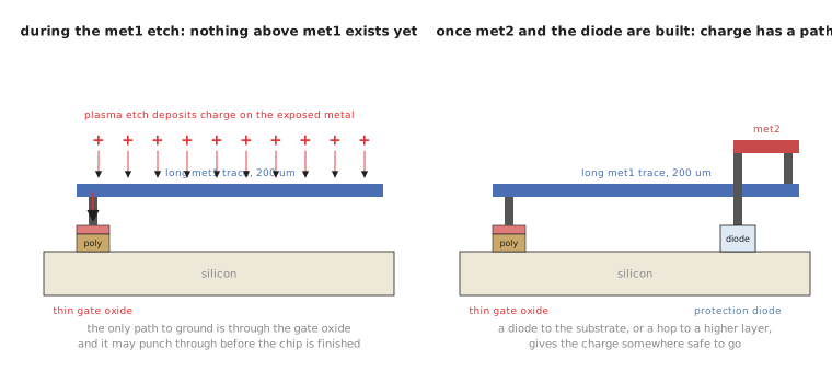
If enough charge builds on a long exposed piece of metal with nowhere to go, the voltage can rise far enough to punch through and permanently damage the thin gate oxide it is connected to. Silent damage that may not show up until the finished chip is tested and a gate that should work is degraded or dead.
Why this is a routing preview and not a layout curiosity
The geometry that creates antenna risk is created during routing. A net’s risk scales with how much conductive area is connected to a sensitive gate on one layer before a via up to a higher layer, or a protection structure, breaks that exposure. In practice, long traces on a single layer, especially lower layers built early, are the geometry to watch. A short hop from a driving cell to the next cell over is essentially never a problem. A long single-layer run crossing a meaningful fraction of the die before it changes layers or reaches a diode is exactly the shape antenna rules exist to catch.
That is why the preview belongs here. The decisions that create or avoid antenna risk, how long a trace runs on one layer before hopping up, whether a net is broken across layers or held on one, are routing decisions, even though checking and fixing, jumper insertion and protection diodes, is Module 8’s job. OpenLane runs an antenna check as part of its signoff sequence, and the fixes it applies are exactly the ones Module 8 walks through. What matters now is recognising the shape of the risk.
It is an unintuitive kind of problem. It is not visible in a schematic, not caught by simulation, not a timing problem, and not even a routing DRC violation of the spacing or width kind. It is purely a geometric by-product of how a net was routed, checked by a separate rule class layered on top of everything else in this module.
Spotting the riskiest net
Before you have seen any antenna ratio, use the intuition above. Four nets from the routed UART, with their approximate single-layer run before reaching a via to another layer or the gate they drive:
| Net | Single-layer run before via or gate | Driven structure |
|---|---|---|
baud_tick |
3 um on met1, then vias up to met3 | Clock-gate enable input |
tx_data[4] |
180 um on met2, no layer change for most of it | Shift register data input |
rx_start_bit |
8 um on met1, then vias up to met2 | Input to a small combinational decoder |
reset_n |
210 um on met3, no layer change for most of it | Reset input on dozens of flops |
reset_n looks like the highest risk: the longest single-layer run with nothing breaking up the exposed area, fanning out to dozens of gate inputs, so a lot of connected gate area is exposed to whatever charge that trace collects. tx_data[4] is next for the same reason, shorter and with less gate area. baud_tick and rx_start_bit both change layers early, which is the kind of geometry that tends to be lower risk. This is intuition rather than the ratio calculation Module 8 does, but it is the right instinct: long, single-layer, high-fanout nets are the ones to look at twice.
Practice Exercise
A routing engineer proposes eliminating antenna risk by avoiding long single-layer runs altogether, routing every net so it changes layers every few microns. What is a plausible downside, tying back to what you learned about vias?
Solution
Every layer change is a via, and vias are not free. They consume routing resources, add resistance and a little delay compared with a straight run, and each one has to satisfy enclosure and spacing rules in whatever local geometry it lands in. Forcing a layer change every few microns on every net would multiply the design’s via count, creating new spacing and enclosure violations in tight regions and adding resistance to nets that did not need it, trading a fabrication risk on some nets for a congestion and timing cost on all of them. The real fix in Module 8 targets only the nets actually at risk.
Spacing, width and antenna rules all live inside one much larger document, the DRC rule deck. The next article looks at the actual shape of a rule deck entry.