Spacing and Width Rules
Section 6.3 is about the rulebook. TritonRoute reported zero violations on the UART’s routing run, and behind that clean report is the SKY130 design rule deck, which told the router exactly how close two wires may get and how thin a wire may be on every layer. This article is about where those two rule families come from, because “the tool enforces it” is a much weaker understanding than “here is the physical reason the rule has to exist”.
Width rules: what the process can actually print
A layout is a design intent, a rectangle you drew meaning “put metal here”. Fabrication is the process of depositing and etching that metal on a real wafer, and it has physical limits on how small a feature it can reproduce. Ask for a wire narrower than the process can resolve and you do not get a thin wire. You get an unpredictable one: sometimes it prints, sometimes thinner than intended, sometimes not continuously at all, silently breaking a connection that looked fine in the viewer.
Minimum width rules keep every drawn shape inside the region where the process behaves predictably. They are layer-specific because each layer is patterned with different steps and different achievable resolution, which is why the lower layers, closer to the transistors and patterned with the tightest, most expensive steps, support finer minimum widths than the layers near the top. met1’s minimum width is tighter than met4’s or met5’s, mirroring the pitch relationship from the metal stack article.
Spacing rules: shorts the process cannot guarantee against
Minimum spacing rules solve the opposite failure. Two wires that should stay electrically separate need enough physical distance between them that ordinary manufacturing variation, a slightly misaligned mask, a slightly over-etched feature, cannot bridge them into a short or erode one into an open. Spacing rules are the process saying “guarantee this much daylight and I can guarantee these two shapes will not merge”.
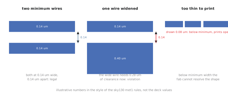
The detail that trips people up the first time: minimum spacing is often not one flat number per layer. Real decks specify spacing as a function of the width of the shapes involved. Wider wires frequently need more clearance than two minimum-width wires need from each other. Intuitively, a wider shape casts a bigger shadow for etch and lithography variation to act on, so the safe margin around it scales up too. You will see exactly this expressed as two separate entries in a real deck two articles from now.
That is also why detailed routing sometimes gives a long, wide net, a bus carrying real current or a net deliberately widened for resistance, more clearance than a minimum-width neighbour would get. The router is not being cautious for no reason. It is satisfying a conditional rule. And it is why a design can pass DRC everywhere except around one unusually wide wire. The rule did not change; the threshold that applies to that shape did.
Compliant or not, by reasoning
Take a qualitative rule: on this layer, spacing between two shapes has a flat baseline when both are at or near minimum width, but the required spacing increases once either shape’s width exceeds a threshold. Two scenarios. First, two minimum-width signal wires at the baseline spacing. Second, one of those wires widened, say because it was merged with a parallel wire to cut resistance, with the spacing to its neighbour left unchanged.
The first is compliant by construction. The second is very likely not. Widening past the threshold triggers the larger spacing requirement, but the gap was left at the old baseline. The fix is not to shrink the wire back, which defeats the reason it was widened. It is to move the neighbour further away or reroute one of the two so the clearance is legal for the new width.
Practice Exercise
A teammate widens a power strap on met4 to reduce IR drop, touching nothing else nearby. TritonRoute later reports new spacing violations against that strap that were not there before. Explain what almost certainly happened in terms of the two rule families.
Solution
Widening the strap pushed it past the width threshold where met4’s spacing requirement steps up. The old spacing to neighbouring wires was legal for the strap’s original width and is no longer legal for its wider self. It is not a width violation, the strap is fine at its new width. It is a spacing violation triggered by the width change, exactly the second-order effect that makes “just widen it a bit for IR drop” a change that needs a routing recheck rather than a one-line edit assumed safe.
Spacing and width rules protect against shorts and unreliable prints in the finished chip. The next article previews a rule that protects against damage that happens during fabrication, before the chip is even finished: the antenna effect.