The SKY130 Metal Stack
Open a routed layout in KLayout for the first time and it looks like abstract art: stacked rectangles in half a dozen colours, some hair-thin, some fat, some running the whole width of the die. It is tempting to treat that as decoration. It is not. Every colour is a physical layer of deposited metal with its own thickness, resistance and, critically for you, its own conventional job. Learn the stack once and every routing report, DRC violation and congestion map in this module stops being noise.
Why there is a stack at all
A single layer of metal cannot route a modern digital design. With thousands of cells and tens of thousands of nets, wires would have to cross constantly, and metal on the same layer cannot cross without shorting. The fix is to stack several layers, each carrying wires, connected to each other and to the transistors below through vertical contacts and vias. Wires on different layers cross freely as long as they do not need to connect. That is what a layer buys you: crossing without touching.
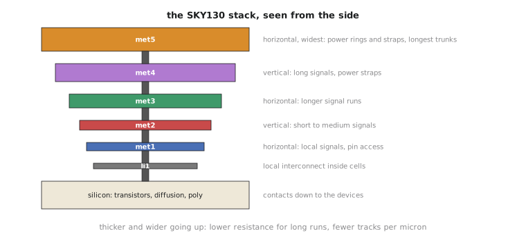
SKY130’s standard cell stack, the configuration OpenLane targets with sky130_fd_sc_hd, has five metal layers plus a local interconnect layer under them. From the transistors up:
What each layer is conventionally for
| Layer | Conventional role | Typical net length | Notes |
|---|---|---|---|
| li1 (local interconnect) | Connecting transistors and pins inside a standard cell, and very short hops to an adjacent cell | Sub-cell to a few cell pitches | Below met1; mostly the cell library’s own internal wiring, used by the router for pin access rather than general routing |
| met1 | Local signal routing between neighbouring cells, and pin access | Short, within a row or two | Finest pitch of the general routing layers; the layer detailed routing leans on hardest for dense local connections |
| met2 | Short to medium signal routing, in the other direction from met1 (routers alternate preferred direction layer by layer) | Medium | Works with met1 as a pair for most cell-to-cell wiring |
| met3 / met4 | Longer signal runs across the design, and increasingly power strap segments as you go up | Medium to long | Wider tracks, more resistance-tolerant, suited to nets that travel far |
| met5 | Power distribution, rings and straps, and the longest global trunks | Long, chip-spanning | Widest, lowest resistance per square; reserved mostly for the power grid built in Module 3 |
Notice the pattern: pitch gets coarser and wires get wider as you go up. That is a direct consequence of resistance. A signal travelling the width of the die on a thin, high-resistance layer would suffer enough RC delay to blow through its timing margin the moment it left the driving cell. Wider, higher metal has lower resistance per unit length, so it is the natural home for long runs, which is exactly why the power grid, which has to deliver current across the whole die with minimal IR drop, lives at the top.
OpenLane exposes this choice directly through RT_MIN_LAYER and RT_MAX_LAYER, which bound the layers the global and detailed routers may use for signals. A UART-scale design might set them to met1 and met4, deliberately reserving met5 for the power straps so the router never fights the grid for space on the layer the grid needs.
The instinct to resist is “every net should use the highest layer available, because higher metal is better”. Higher metal is lower resistance but far scarcer. Every layer above met2 has progressively less total track capacity, because power straps and long clock and global nets already claim a share. Routing short local nets on met4 because it is there wastes capacity that longer nets need. That is exactly the instinct track assignment, in the next article, exists to correct.
Picking a layer from the role
For each net below, pick the most plausible layer from the table, reasoning about role rather than computing anything.
| Net | Approximate span |
|---|---|
baud_gen_q[2] to the adjacent flop’s D input, same row |
1 to 2 cell pitches |
tx_data[7:0] bus feeding the shift register, about a third of the core width |
Medium |
VPWR ring around the whole core |
Full die perimeter |
baud_gen_q[2] to the adjacent flop: met1, perhaps li1 for the last stretch into the pin. This is exactly the short, local hop met1 is for. tx_data[7:0] at a third of the core: met2 or met3, too long to be comfortable on met1’s fine, resistive tracks, not long enough to justify climbing to met4 or met5 and competing with power and global routing. VPWR around the whole core: met4 or met5, precisely the long-run, low-resistance, high-current job the top of the stack exists for, and it matches the ring you built in Module 3.
Practice Exercise
A congestion report flags met2 as the most congested layer in the design, with met4 nearly empty. You suspect the netlist has an unusually large number of medium-length nets. Before touching placement or floorplan, what routing knob from this article could you try, and what is the risk of pushing it too far?
Solution
Adjust the layer bounds or layer preference so some of the medium traffic forced onto met2 moves up to met3 and met4 where there is spare capacity. The risk is that pushing too much upward starts competing with the power straps and any long global nets that specifically need those layers for their resistance. You would be solving met2 congestion by creating a met4 IR-drop or long-net delay problem. Layer bounds are a real lever, but they trade one layer’s congestion for another’s, not free capacity.
Now that you know which layer a net’s rough path should live on, you need to know how that rough path becomes an exact track. That is track assignment, the next article.