Cell Flipping and Row Alignment
Look at any row of standard cells side by side: a VDD rail along the top edge, VSS along the bottom, and a rail shared by every abutting cell so power does not need a separate wire per cell. Now stack a second row directly above the first. If both rows have VDD on top, the lower row’s VDD rail and the upper row’s VSS rail sit right against each other at the boundary. Different nets, physically adjacent, exactly what a DRC check exists to catch.
The fix is architectural rather than a workaround: every other row is flipped top to bottom. Row 1 sits in its normal orientation, N. Row 2 is flipped vertically, FS. Row 3 is back to N, and so on. Flip a row and its rail order reverses, so every row boundary becomes a rail-to-rail match, VDD meeting VDD and VSS meeting VSS, and adjacent rows share one physical rail instead of each needing its own.
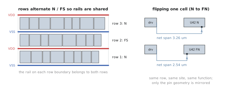
Read the boundary between row 3 and row 2 in the figure: VSS at the bottom of row 3 meets VSS at the top of row 2, because row 2 is flipped. Between row 2 and row 1, VDD meets VDD. This scheme is standard in every standard-cell flow, not an OpenLane quirk, and it is set up automatically once the floorplan defines the rows.
Flipping individual cells
Row orientation is a floorplan-level, whole-row decision. Detailed placement has a second, finer trick on top of it: it can mirror an individual cell left to right (N to FN, or FS to S, in DEF orientation notation) without moving it off its row or site. A NAND2 is still a NAND2 after mirroring, but its pin locations move, because the mirror swaps left-side geometry for right-side geometry.
If a cell’s input pin currently faces away from the cell driving it, flipping the cell puts the pin on the right side and shaves real distance off that net, for free, because the cell does not relocate.
Take a two-input gate U42 at x = 20.0 um. Its input pin A is currently on the cell’s east edge at x = 20.36 um. The cell driving pin A sits at x = 17.10 um, to the west.
- Current orientation: pin
Aon the east edge at 20.36 um. Net span = 20.36 - 17.10 = 3.26 um. - Flip
U42horizontally: pinAmoves to the west edge, at about 19.64 um (mirrored across the cell’s own width of roughly 0.72 um). Net span = 19.64 - 17.10 = 2.54 um.
Flipping this one cell, with no relocation, same row and same site, shortens the net’s HPWL contribution from 3.26 um to 2.54 um. Across a design with thousands of cells, this class of free, local pin-side correction is a meaningful part of what detailed placement does after legalisation settles the rows. It is also why detailed placement and legalisation are usually described as one phase even though they are distinct jobs. A legaliser that only snapped cells to rows and stopped would leave cheap wins like this on the table.
Flipping is not free in every sense, though. It is free in area and in position, but it moves every pin on the cell, not only the one you are looking at. A flip that helps one net can hurt another net on a different pin of the same cell. Detailed placement weighs the net effect across all of a cell’s connections before committing.
Practice Exercise
A buffer has two pins: input A on its west edge and output Y on its east edge. Its driver sits 4.0 um to the west; its load sits 4.0 um to the east. Would flipping this cell help, hurt or do nothing to its total connected wirelength? Explain without arithmetic.
Solution
It does nothing useful. For a cell whose driver and load sit symmetrically on opposite sides, matching its existing pin layout, the current orientation is already the good one. Flipping would put A on the east edge and Y on the west, so the net from the west-side driver would have to reach across the whole cell to A, and the net to the east-side load would reach back across to Y. By symmetry the total length is identical, and nothing is gained. That is the reasoning detailed placement automates: it flips a cell only where the pin-to-neighbour geometry is genuinely suboptimal.
Rows are legal and cells are flipped for local wirelength wins. That is as good as a placement gets without running the tool. The next article does exactly that: run global and detailed placement on this module’s reference design and read the real report.