The LEF File
The previous article covered the timing view of a cell. This one covers the physical view.
Synthesis has just picked sky130_fd_sc_hd__nand2_1 over nand2_2 because Liberty said so. Hand that netlist to a placer and it asks a different question: how wide is this cell, and where on its boundary does pin A sit, so a wire can be routed to it? Liberty has no answer; it was never designed to. That lives in LEF, the Library Exchange Format.
Two views of the same cell
Liberty (.lib) |
LEF (.lef) |
|
|---|---|---|
| Describes | Timing, power, logical function | Physical footprint, pin locations, blockages |
| Used heavily by | Synthesis, STA | Floorplanning, placement, routing |
| Answers | “How fast, how much load, what logic?” | “How big, where are the pins, what is off-limits?” |
| Units | Time (ns), capacitance (pF), power | Distance (µm), on a fixed routing grid |
This module barely touches LEF operationally, since synthesis runs on Liberty alone, but the netlist this module produces is the input Module 3’s floorplanner and Module 4’s placer consume, and those tools care about LEF far more than Liberty. Meeting it now means Module 3 is not introducing a file format cold.
Reading a cell’s LEF entry
A representative entry, in the structure of real LEF, for the same NAND2:
MACRO sky130_fd_sc_hd__nand2_1
  CLASS CORE ;
  SIZE 5.750 BY 2.720 ;
  SYMMETRY X Y ;
  PIN A
    DIRECTION INPUT ;
    PORT
      LAYER li1 ;
        RECT 0.310 0.700 0.470 2.020 ;
    END
  END A
  PIN Y
    DIRECTION OUTPUT ;
    PORT
      LAYER li1 ;
        RECT 4.900 0.700 5.060 2.020 ;
    END
  END Y
  PIN VPWR
    DIRECTION INOUT ;
    USE POWER ;
  END VPWR
  PIN VGND
    DIRECTION INOUT ;
    USE GROUND ;
  END VGND
END sky130_fd_sc_hd__nand2_1
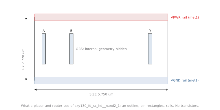
Field by field:
SIZE 5.750 BY 2.720: the cell occupies a 5.750 µm by 2.720 µm rectangle. Every cell in a library shares the same height (2.720 µm here), which is what lets standard cells snap into uniform placement rows, a fact Module 3 leans on directly.- Pin
A’sRECT: a rectangle on layerli1, given as lower-left x, lower-left y, upper-right x, upper-right y, relative to the cell’s origin. This is the physical location a router must land a wire on to reach inputA. PIN VPWRandPIN VGND: power and ground, markedUSE POWERandUSE GROUNDrather than being ordinary signal pins. Module 3’s power planning comes back to this.
The same cell looks radically different in its two files. Liberty’s entry had no concept of “5.750 µm wide”; LEF’s has no concept of “0.0421 ns delay”. Neither is incomplete. Each is deliberately narrow, tuned to the class of tool that reads it. And a bigger drive-strength variant (next article) is directionally a wider cell in LEF terms, but the LEF size and the Liberty area come from different characterisation processes and should not be treated as interchangeable without checking both.
Practice Exercise
A LEF entry for another cell reads SIZE 8.050 BY 2.720 ;. Compare with the NAND2 above and state what you can and cannot conclude from that comparison alone.
Solution
You can conclude the second cell is wider (8.050 versus 5.750 µm) with the same row height (2.720 µm), so both fit the same placement rows. You cannot conclude why it is wider or what it costs in delay or power; that needs the same cell’s Liberty entry. A wider cell might be a higher drive-strength buffer (more transistor width, next article), a more complex compound gate with more transistors, or a cell with more pins needing room for pin access. SIZE alone does not distinguish these.
Standard cells rarely come in one size per function. A real library offers several drive-strength variants of the same gate. In the next article we look at why, and how to pick one for a given load.