Technology Mapping
Module 1 ran synthesis as the first stage of the flow without opening it up. This module does, and the first thing to understand is the step at the very end of synthesis.
When Yosys reads your Verilog and eventually emits a netlist full of sky130_fd_sc_hd__nand2_1 and sky130_fd_sc_hd__mux2_1 instances, how did it know those cells exist? Underneath, synthesis does not think in terms of NAND2 or AND2 for most of its work. It thinks in Boolean algebra, and only converts to real cells at the last step. That step is technology mapping.
Two jobs, one tool chain
Synthesis is two jobs joined together:
- Logic optimisation: take the RTL’s Boolean behaviour and simplify it: remove redundant logic, factor shared terms, restructure for fewer levels. This happens on a generic, technology-independent representation. Internally Yosys holds the design as a graph of primitive operations (AND, OR, NOT, XOR, MUX) with no concept of cell area or drive strength.
- Technology mapping: take that optimised network and match its pieces onto the gates a specific library provides, picking the combination that best satisfies the goal (area, delay, or a mix).
In OpenLane, job 1 is Yosys’s own passes; job 2 is delegated to ABC, a logic synthesis and mapping engine from UC Berkeley that Yosys calls with the library’s Liberty file as the menu of available parts.

Why split it this way instead of mapping straight to real cells? Because a generic network is much easier to optimise. The optimiser does not have to think about which of five NAND2 drive-strength variants to use while it is still deciding the logical structure. Structure first, parts second. The third article in this section comes back to this from the tool’s side.
Mapping is a matching problem, not a lookup
The word “mapping” undersells the choice involved. Technology mapping is a covering problem: ABC breaks the network into small subgraphs and searches for combinations of library cells whose combined function exactly covers each one, then picks the covering that minimises its cost function (area, delay, or a blend, depending on the strategy in Section 2.2).
There is almost never exactly one right answer. The same function can be built from very different gate combinations, and a real library gives ABC dozens of legal ways to cover the same logic. That is the thing to internalise before touching a tool: two synthesis runs of identical RTL with different priorities can and should produce different netlists that are both correct. A netlist is not “the” translation of your RTL into gates; it is “a” translation, one of many that are functionally identical and physically different.
Hand-map a small expression
Let us do by hand what ABC does automatically at a much larger scale. Suppose the library is stripped down to four gates:
| Cell | Function | Illustrative area (units) |
|---|---|---|
| INV | Y = NOT A |
1 |
| AND2 | Y = A AND B |
2 |
| OR2 | Y = A OR B |
2 |
| NAND2 | Y = NOT (A AND B) |
1.5 |
The function to map:
$$ F = (A \cdot B) + \overline{C} $$
that is, F = (A AND B) OR (NOT C). Figure 2 shows two valid mappings.
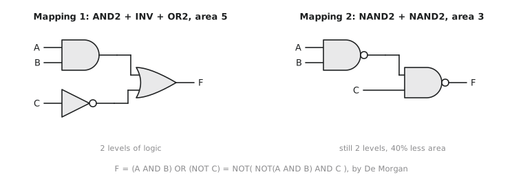
Mapping 1, the direct structural match: one AND2 for A AND B, one INV for NOT C, one OR2 to combine them. Area 2 + 1 + 2 = 5 units, two logic levels.
Mapping 2, a NAND-based restructuring: by De Morgan, (A AND B) OR (NOT C) equals NOT(NOT(A AND B) AND C), which maps onto two NAND2 gates with no separate inverter. Area 1.5 + 1.5 = 3 units, still two levels. Smaller and no slower: a strictly better mapping for this library, and exactly the kind of restructuring ABC searches for across a library with dozens of cells and thousands of possible coverings.
A synthesis tool that restructures your logic into a different gate topology while preserving its Boolean behaviour is not malfunctioning. That is the whole point of technology mapping, and the netlist that looks closest to your RTL is not the “real” one.
Practice Exercise
Using the same four-cell library, hand-map F = NOT(A OR B) two different ways, and say which is cheaper by the area column.
Solution
Mapping 1, direct: OR2 followed by INV. Area 2 + 1 = 3 units, two levels.
Mapping 2: there is no NOR2 in the toy library, but by De Morgan NOT(A OR B) is NAND(NOT A, NOT B), which needs two INVs plus a NAND2. Area 1 + 1 + 1.5 = 3.5 units, still two levels since the INVs are in parallel.
Mapping 1 is cheaper, 3 against 3.5, precisely because the toy library lacks a NOR2, which a real library would supply for this function at lower cost than either option. The practical point: the best mapping depends entirely on what the library contains, not on an abstract ideal.
Technology mapping does not only care about the library. It cares just as much about how the RTL was written. In the next article we look at why two logically equivalent always blocks can synthesize to structurally different, and differently placeable, netlists.