Module 7: Advanced RTL Design Techniques
Module 5 gave us the behavioral constructs and Module 6 gave us the testbenches to prove a design works. By now you can write correct RTL. This module is about the gap between correct and shippable, which in my experience is where most of the real work is.
An 8-bit adder that only works at 8 bits gets copy-pasted, not reused. A datapath that cannot meet the clock target does not tape out. A FIFO that assumes both sides share a clock corrupts data the day it is used between two clocks. A design that toggles every flip-flop on every cycle gets sent back from the first power review. Module 7 covers the patterns that fix each of those, and they are patterns you will meet in nearly every ASIC or FPGA project.
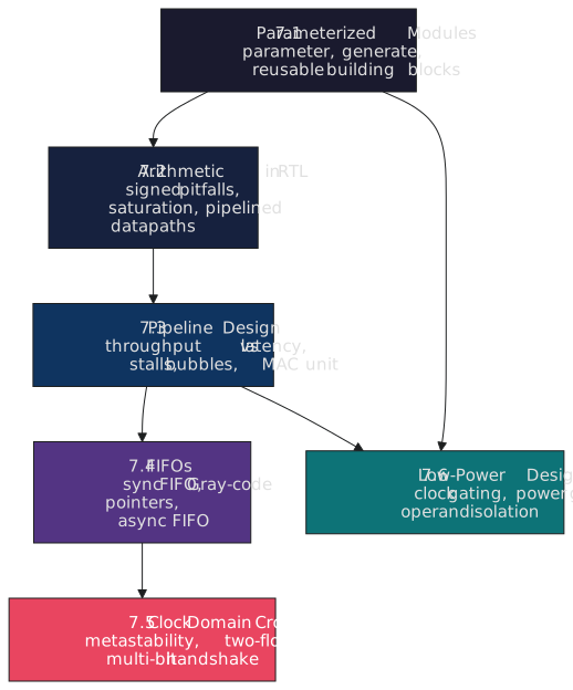
Sections 7.1 and 7.2 make the RTL you already know how to write reusable (parameters, generate) and correct at the edges (signed arithmetic, saturation). Section 7.3 pipelines that arithmetic to meet a real clock. Section 7.4 builds the FIFO, probably the most instantiated block in digital design, and along the way meets Gray code. Section 7.5 makes the clock domain crossing theory that the FIFO quietly depends on explicit. Section 7.6 closes with the power techniques that matter the moment a design has to run from a battery.
What we will build
| Design | Section | What it teaches |
|---|---|---|
| Parameterized N-bit memory model | 7.1 | Width-configurable RTL with parameter and generate |
| Saturating signed adder | 7.2 | Signed arithmetic pitfalls, saturation logic |
| 2-stage pipelined multiplier | 7.2 / 7.3 | Breaking a long combinational path into registered stages |
| Pipelined multiply-accumulate (MAC) unit | 7.3 | The standard pipelining worked example |
| Synchronous FIFO | 7.4 | Full/empty flag generation, pointer arithmetic |
| Gray-code pointer pair | 7.4 / 7.5 | Safe multi-bit values crossing clock domains |
| Asynchronous FIFO | 7.4 | The most common CDC structure in real chips |
| Two-flop synchronizer | 7.5 | The single-bit CDC primitive |
| Multi-bit handshake synchronizer | 7.5 | Request/acknowledge crossing between clock domains |
| RTL-inferred clock gate | 7.6 | The only safe way to gate a clock |
Every design comes with a self-checking testbench, as in the earlier modules.
Objectives by section
| Section | You will be able to |
|---|---|
| 7.1 Parameterized Modules | Write width-agnostic RTL with parameter, use generate if/generate case for structural variation |
| 7.2 Arithmetic in RTL | Avoid the signed keyword’s traps, implement saturating arithmetic, identify what needs pipelining |
| 7.3 Pipeline Design | Insert pipeline registers correctly, track data validity, reason about stalls and bubbles |
| 7.4 FIFOs | Build a correct synchronous FIFO, explain why Gray code is required for CDC pointers, build an asynchronous FIFO |
| 7.5 Clock Domain Crossing | Apply the two-flop synchronizer correctly, design a multi-bit CDC handshake, name the mistakes CDC lint tools catch |
| 7.6 Low-Power Design | Explain clock gating, power gating and operand isolation, and know why you never gate a clock by hand |
Estimated time
| Section | Posts | Reading and exercise time |
|---|---|---|
| 7.1 Parameterized Modules | 4 | ~48 minutes |
| 7.2 Arithmetic Circuits in RTL | 4 | ~52 minutes |
| 7.3 Pipeline Design | 4 | ~56 minutes |
| 7.4 FIFOs | 5 | ~72 minutes |
| 7.5 Clock Domain Crossing | 4 | ~56 minutes |
| 7.6 Low-Power Design Techniques | 4 | ~44 minutes |
| Total | 25 | ~328 minutes |
Section 7.1 starts with something you have probably already done without naming it: copying the same adder into three projects at three widths. The fix is a keyword you already know, parameter, used with more discipline than we have needed so far. Start with 7.1 Parameterized and Scalable Modules.