Clock Gating and the ICG Cell
Section 7.5 finished the clock domain crossing material. Section 7.6 is about power, and it starts with the clock, because the clock is the highest-toggling net in the chip.
Section 5.5 said never to write assign gated_clk = clk & en; yourself, and promised the tool would insert something safer if you described the enable behaviourally. This article opens up what that something is, and why it has to exist rather than just being a tidier AND gate.
The glitch hazard, precisely
clk & en is a combinational AND gate in a clock path. If en changes at a moment when clk is already high, the gate’s output can produce a runt pulse, a clock edge too short for downstream flops to capture data reliably, or a spurious extra edge that nothing in the design intended. Every flop on that gated clock is now exposed to a hazard that static timing analysis was never built to catch, because STA assumes clock paths are clean by definition.
The ICG cell: a latch in front of the gate
The fix that standard cell libraries provide is the integrated clock gating (ICG) cell, and its defining feature is a transparent latch ahead of the AND gate:
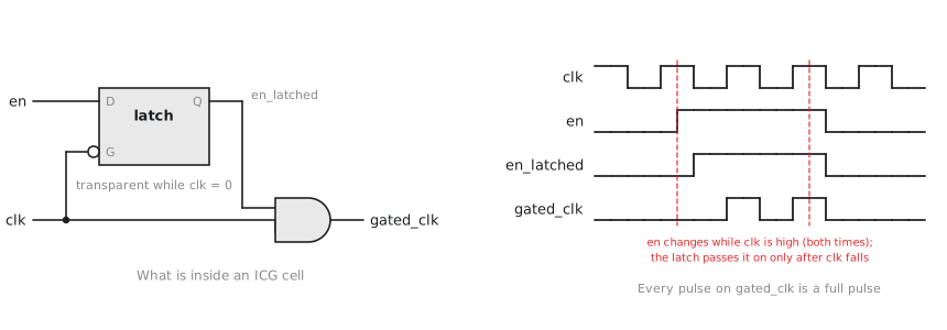
The latch is transparent only while clk is low, and holds while clk is high. That one detail is the whole fix. en can only change the latch’s output during the half of the cycle when clk is already low, so by the time clk rises, en_latched has settled and cannot change mid-pulse. The AND gate combines a clean clk with an en_latched that is guaranteed stable for the whole time clk is high, which removes the runt-pulse and spurious-edge hazards the bare AND gate cannot avoid. If en changes while clk is high, the latch simply holds; the change appears on en_latched at the next low phase. Figure 1 shows both cases.
RTL that synthesis recognises as clock gating
You never instantiate an ICG cell in behavioural RTL. You describe the enable pattern, as in Section 5.5, and let synthesis recognise it and map it onto the library’s ICG cell:
always @(posedge clk or negedge rst_n) begin
    if (!rst_n)
        data_reg <= {WIDTH{1'b0}};
    else if (en)
        data_reg <= data_in;
    // else: data_reg holds. This is the pattern the tool recognises.
end
Modern synthesis tools recognise this across a whole register bank sharing the same enable and clock, and consolidate the enable into a single ICG cell driving a shared gated clock net, rather than one ICG per flop. That is a much bigger win than gating registers individually, because the entire clock tree downstream of that one cell stops toggling whenever the shared enable is low.
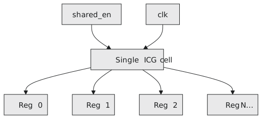
Whether your tool does this consolidation on its own, or whether you need to make the shared enable more visible (grouping registers that share an enable into one always block or one module), is worth checking in the tool documentation. The opportunity is the same either way: one gated clock net serving many registers beats one per register, because it is the clock tree, not only the flops, that stops toggling.
In a modern SoC the clock tree can be a third or more of dynamic power, because the clock switches every cycle whether or not anything useful is happening downstream. Clock gating attacks that cost at its source: if a register bank is not going to load new data this cycle, there is no reason for its local clock tree to keep toggling.
Practice Exercise
Using the ICG cell’s latch structure, explain why a design whose enable toggles on every clock cycle (enabled, disabled, enabled, disabled) gets almost no power benefit from clock gating, even though the ICG cell is working correctly.
Solution
If en toggles every cycle, the gated clock is on for roughly half the cycles and off for the other half, so the downstream clock tree still switches on about half of all edges. The savings from clock gating come from sustained periods with nothing to load: the longer the enable stays low, the more consecutive edges are suppressed and the larger the saving. A rapidly alternating enable captures almost none of that. The cell is doing exactly what it is designed to do; this activity pattern just gives it no opportunity to help.
A bare AND gate in a clock path is dangerous because an enable changing while the clock is high produces a runt pulse or a spurious edge. An ICG cell fixes this with a latch that only lets the enable change during the clock’s low phase. You write the ordinary enable pattern and synthesis maps it to the cell, ideally one cell per register bank. In the next article we look at power gating, which cuts power to a block entirely rather than only stopping its clock.