SKY130, Concretely
The previous article explained what a PDK is in general. This one is about the specific PDK we use.
There is a version of this course that could have taught physical design against a fictional, simplified process: three metal layers, made-up spacing rules, nothing that maps to anything real. It would have been easier to write and to teach. It would also have quietly misled you about what this discipline feels like, because real physical design is defined by working with a real, specific, sometimes annoying set of manufacturing constraints that do not go away just because you understand the concept behind them. SKY130 is real. That is the whole reason it is the process this course uses.
What SKY130 is
SKY130 is SkyWater Technology’s open-source 130 nanometre process. “130 nm” names the process generation rather than one literal transistor dimension. It is a mixed-signal process, supporting both digital logic and analog circuitry, with multiple supply voltage domains, which matters for I/O and mixed-voltage designs (touched on here, but not the focus, since this course is about digital physical design).
What makes SKY130 unusual and useful is that SkyWater released its actual design rules, the real DRC and LVS deck a real tapeout uses, as open data, together with a real, fabricable standard cell library. That is different from an educational simplification. It is the real thing, opened up. And 130 nm is a good learning target: modern enough that its rules and metal stack behave like a contemporary digital flow, old enough that the rules are comparatively forgiving to learn on, and open enough that this course can show real commands against a real deck.
One thing this course will not do is hand you a specific numeric DRC value, an exact minimum spacing in nanometres, and ask you to memorise it. Real rule values live in the SKY130 deck files, and they are more useful looked up in context, against real tool output, than memorised in the abstract. Where a number is useful for a worked example, treat it as illustrative. The DRC articles in Module 8 are where you work against the real deck.
The metal stack, bottom to top
Every routed design sits on a stack of interconnect layers, and SKY130’s stack has a specific named structure worth learning now because Module 6 depends on it.
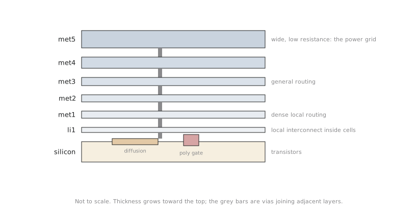
- li1, local interconnect, sits closest to the transistors. It is the first level of wiring above the active silicon, used for very short connections inside and immediately around a standard cell.
- met1 through met5 are the general routing layers, met1 nearest the transistors and met5 at the top.
- The top layers are conventionally reserved for the widest, lowest-resistance routing, which is why the power grid you build in Module 3 runs on the upper metal layers while dense local signal routing concentrates on the lower ones.
This “local connections low, power distribution high” pattern is not SKY130-specific. It is near universal, because lower layers are physically thinner and higher-resistance, suited to short dense wiring, while upper layers are thicker and lower-resistance, suited to carrying the current a power grid needs across long distances.
Placing the stack against what you know
Without opening a tool, answer from Figure 1 alone: if you had to connect two adjacent transistors inside one cell, which layer would you expect that connection to use? And if you had to distribute power from a pad to every cell across the die?
The first is what li1 is for: the shortest, most local connections, at the transistor level. The second is what met5 is for: long-distance, low-resistance distribution across the die. You have just predicted, from first principles, the layer assignment pattern Modules 3 and 6 depend on.
More metal layers is not automatically better or faster. More layers give the router more room and more flexibility, but every layer transition, a via, adds resistance and capacitance of its own. Routing is an optimisation problem, not “use as many layers as you can”, which is why Module 6 is a module and not a footnote.
Practice Exercise
A power grid needs to carry significant current across the whole die with minimal resistance. A signal net only connects two adjacent cells a few microns apart. Predict which layer each would most likely use, with one sentence of justification each.
Solution
The power grid would most likely use met5 (or another of the top layers), because the top layers are the widest and lowest-resistance, exactly what a die-wide, high-current net needs. The short signal net would most likely use li1 or met1, because it spans only a few microns and using an upper layer for it would spend a scarce, high-value routing resource and add unnecessary vias for a connection that does not need the low resistance. Matching a net’s electrical requirement to the layer whose properties fit it is the judgement both Module 3’s power planning and Module 6’s routing build on.
SKY130 does not ship as one standard cell library. In the next article we cover the hd, hs and ls variants, and how OpenLane picks one per design.