Why Physical Design Is Not Optional
The previous article showed that speed is not visible at the RTL layer. This one lists everything else that is not.
There is a sentence every RTL engineer eventually hears from a physical design team, usually with some frustration attached: “Your design passes every test, and it doesn’t work.” Not a logic bug, not a missed corner case. The RTL is, by every front-end measure, correct, and the chip still cannot ship. That is not a contradiction. It is the reason physical design is a separate, mandatory discipline rather than something bolted on after RTL signoff. Four things can independently sink a functionally perfect design, and none of them is visible from inside a testbench.
Four ways to fail after passing every test
Timing. An RTL testbench simulates with zero wire delay and idealised gate delays, if it models delay at all; functional simulation is about correctness, not speed. A common story: a design meets timing comfortably in a pre-layout estimate, gets placed and routed, and the routed wire delay on its longest path comes out 40 percent worse than the estimate assumed, because real wires have real resistance and capacitance that scale with physical distance, and physical distance does not exist until placement. The design that worked cannot reach its target clock.
Area. RTL has no notion of size. A design can implement its specification correctly and still need more gates than, once synthesized and placed at a realistic density, fit inside the die area the package and cost budget allow. There is no bug to fix. The chip as specified cannot be built at the size the business case requires.
Power. A design can work on a lab bench at low switching activity and still fail in the field: heavy current through the power grid causes IR drop severe enough that some cells receive a lower supply than they were characterised for, and they fail timing or behave unpredictably under a particular activity pattern the lab never exercised.
Yield. A design that closes timing, fits its area and manages power can still fail in fabrication if its layout violates the fab’s rules or is needlessly vulnerable to random defects. A fragile layout turns “most dies work” into “very few dies work”.
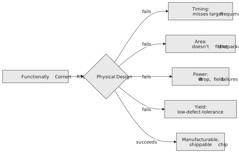
All four share one root cause: they are properties of the physical implementation, and the physical implementation does not exist until physical design creates it. A testbench can only fail a design on axes it measures, and none of these four is measurable at RTL simulation.
The course, stage by stage, is the answer to each
That is the syllabus. Every module from here is aimed at one or more of these:
| Failure mode | Addressed mainly in |
|---|---|
| Timing | Module 2 (synthesis constraints), Module 5 (clock tree), Module 7 (timing signoff) |
| Area | Module 3 (floorplanning), Module 4 (placement density) |
| Power | Module 3 (power planning), Module 8 (IR drop checks) |
| Yield | Module 8 (DRC, LVS, antenna), Module 9 (DFM, GDSII signoff) |
A first physical number
Everything so far has been conceptual. Here is the first physical calculation, a rough die area estimate, the same back-of-envelope arithmetic a physical designer does before any tool runs.
Say a synthesized design has about 20,000 standard cell instances, each occupying on average about 6 square micrometres (a plausible illustrative figure for a small digital cell in a process like SKY130; treat it as illustrative, not a datasheet value). The raw cell area is:
$$ \text{Area}_{\text{raw}} = 20{,}000 \times 6\ \mu m^2 = 120{,}000\ \mu m^2 $$
No real placement fills 100 percent of the area; routing needs room. At a realistic utilisation of 50 percent (cells occupy half the core, the rest is left for routing and margin, a knob you will meet in Module 3 as FP_CORE_UTIL) the core area roughly doubles:
$$ \text{Area}_{\text{core}} = \frac{120{,}000\ \mu m^2}{0.50} = 240{,}000\ \mu m^2 \approx 0.24\ mm^2 $$
That is a real number, a rough estimate of how much silicon the design needs, from nothing but a gate count and an assumed cell size. Module 3 shows how OpenROAD’s floorplanner turns the same reasoning into a die outline. Utilisation targets in the 40 to 60 percent range are common starting points; push utilisation too high and the router may not have room to complete every connection, which is its own failure, covered in Module 6.
Practice Exercise
A design has 8,000 standard cell instances averaging 4 µm² each. Using a target utilisation of 40 percent, estimate the core area in mm².
Solution
Raw cell area: $8{,}000 \times 4\ \mu m^2 = 32{,}000\ \mu m^2$.
Core area at 40 percent: $32{,}000 / 0.40 = 80{,}000\ \mu m^2 = 0.08\ mm^2$.
Lowering the utilisation target (more room for routing) directly increases the estimated area for the same logic, a trade you will manage with FP_CORE_UTIL from Module 3 on.
In the next article, Section 1.2 introduces the open-source tools behind every stage on the map, starting with Yosys and OpenROAD, which turn today’s abstract stage names into runnable commands.