The Abstraction Stack
The previous article drew the line between front-end and back-end. This one names the layers a design passes through on the way down.
Ask an RTL engineer to describe a design and you hear about registers, always blocks and clock domains. Ask a physical designer to describe the same design and you hear about placed cells, wire capacitance and routing congestion. Neither is wrong. They are looking at the same object through different layers of one abstraction stack, and each layer deliberately hides the details that would make its own job impossible. Nobody designs a 50,000-gate block by reasoning about transistors, and nobody manufactures a chip by asking the fab to interpret always @(posedge clk). This article names every rung, because the rest of the course spends nine modules moving down the ladder one rung at a time.
Five layers, one design
| Layer | Expressed in | Question it answers | What it hides |
|---|---|---|---|
| RTL | Registers, combinational logic, clock edges | “What does this do, cycle by cycle?” | Everything physical: no size, no delay, no wires |
| Gate-level netlist | Named standard cell instances plus wires | “What gates implement this, and how are they connected?” | Location, wire length, real delay |
| Placed and routed layout | Cells at (x, y), wires as routed metal shapes | “Where does everything sit, and how is it connected in space?” | The RTL intent: a placed AND gate looks nothing like assign y = a & b; |
| Mask polygons | Geometric shapes per fabrication layer | “What exactly does the fab etch, on which layer?” | Any notion of logic: a polygon does not know it is part of an AND gate |
| Transistors on silicon | Doped regions, oxide, metal contacts | “What physically switches current?” | Nothing; this is the ground truth every layer above describes |
Each step down adds information the layer above lacked and loses a kind of readability the layer above had for free. RTL is easy to reason about precisely because it hides gate count, timing and area. Mask polygons are precise enough to manufacture from precisely because they carry no information about what the design is for. “Abstraction” here does not mean less real. A gate-level netlist is exactly as real a description of the design as the GDSII; it is real about connectivity instead of geometry.
One AND gate, five descriptions
Take the simplest circuit, a 2-input AND gate, y = a & b, and follow it down. No tools needed.
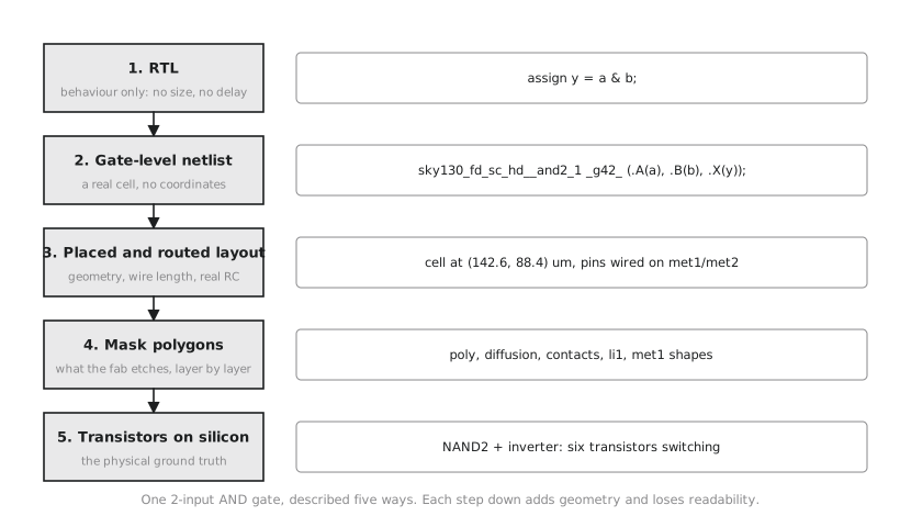
Layer 1, RTL: assign y = a & b;. Pure behaviour, no hint of implementation.
Layer 2, gate-level netlist: synthesis maps this to one instance of a real cell from the target library, something like sky130_fd_sc_hd__and2_1 _g42_ (.A(a), .B(b), .X(y));. Now there is a specific, characterised cell from the SKY130 library you will meet in Section 1.3, but no coordinates and no wire lengths.
Layer 3, placed and routed layout: that instance sits at a specific coordinate on the die, say (142.6 µm, 88.4 µm), and its A, B and X pins connect to whatever needs them through routed metal1 or metal2 segments with real, measurable length, and therefore real resistance and capacitance.
Layer 4, mask polygons: zoom into the placed cell and “and2_1” stops existing as a concept. What is there is an arrangement of polygons: polysilicon forming transistor gates, diffusion forming source and drain regions, contacts joining diffusion and poly up to local interconnect and metal1, and metal1 shapes forming the cell’s internal wiring and pins.
Layer 5, transistors on silicon: physically an AND gate is not even a single-stage primitive. It is a NAND2 followed by an inverter, six transistors switching current based on the voltages on a and b.
This is why a physical designer can meaningfully say “this AND gate is too slow” or “this AND gate is in a congested area”, statements that are meaningless at the RTL layer where the same logic is assign y = a & b; with no physical properties at all. And it is why the netlist is not “basically layout, just not drawn yet”. A netlist has no notion of distance, so two gates joined by a one-line wire in the netlist can end up on opposite corners of the die with a long, slow route between them, and the netlist itself cannot tell you.
Practice Exercise
An RTL engineer says: “My always @(posedge clk) block is one line, so this register update must be fast.” Using the stack, explain what is wrong with the reasoning and which layer you would have to inspect to know the real answer.
Solution
The reasoning conflates “concise at the RTL layer” with “fast in silicon”, but speed is a physical property that does not exist at the RTL layer; RTL describes behaviour, not delay. One line of RTL can synthesize to a flip-flop driven by a deep combinational cloud, or feeding a net that fans out to dozens of cells and gets routed a long distance during placement, either of which could make that one line the slowest path in the design. Answering “is this fast?” means going down to the placed-and-routed layer (real wire lengths and fanout) and ultimately to timing signoff in Module 7, which combines that geometry with real parasitics to produce a delay. RTL conciseness and physical speed are answers to two different questions at two different layers.
With the stack named, the next article makes the stakes explicit: timing, area, power and yield are physical-layer concerns that a functionally perfect RTL design can still fail completely.