Setup, Hold and the Critical Path
Section 8.2 kept saying “the constraints” without explaining them. Section 8.3 is about timing: what the constraints describe, how to write them, and how to read what comes back.
Module 3 gave us setup time, hold time and clock-to-Q for one flip-flop in isolation. A real chip has millions of flip-flops and an enormous number of paths between them. How does anyone verify that setup and hold hold on every one, for a design too large for any person or any testbench to check exhaustively? The answer is static timing analysis, STA, and it is the last piece connecting Module 3’s single-flop timing to “does this chip run at the clock on the datasheet”.
One path, recalled from Module 3
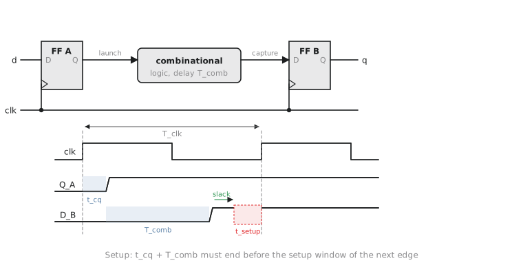
A timing path runs from one flip-flop’s clock edge, through some combinational logic, to the next flip-flop’s data input. Figure 1 shows the path and the corresponding waveforms.
Two conditions, both from Module 3, have to hold.
The setup check: the data arriving at FF B must be stable before the next clock edge, with margin for FF B’s setup time. Within one period $T_{clk}$ the data has to launch from FF A (after its clock-to-Q delay), cross the combinational logic and settle before FF B’s setup window opens:
$$T_{clk} \geq t_{clk-to-Q} + T_{comb} + t_{setup}$$
The hold check: the data must not change too soon after the capturing edge. If the combinational path is too fast, new data can arrive at FF B before it has finished capturing the previous value. This check does not depend on the clock period at all; it is a local, edge-to-edge relationship:
$$t_{clk-to-Q} + T_{comb} \geq t_{hold}$$
The critical path sets the clock
Scale this up. A design has a huge number of these paths, one for every flip-flop-to-flip-flop connection through logic, each with its own $T_{comb}$. The critical path is the single one with the largest setup requirement, the longest $t_{clk-to-Q} + T_{comb} + t_{setup}$ anywhere in the design.
The whole chip’s maximum clock frequency is set by that one path. Every other path could be fast with margin to spare; it does not matter. The period has to be long enough for the slowest path, because a period too short for even one path means that path corrupts data on every cycle.
$$f_{max} = \frac{1}{T_{critical_path}}$$
This is the principle from the stage-balancing article in Section 7.3, generalised from “balance delay across the stages you are designing” to “the chip’s speed is set by whichever single path, out of possibly billions, is slowest”.
Why STA does not simulate anything
This is what makes STA different from every verification technique so far in the course: it never runs a test vector. Functional simulation (Module 6) checks that specific inputs produce specific outputs at specific times, which is useful for correctness but limited to whatever input sequences the testbench applies.
STA instead traces every path through the design’s structure, using only the netlist’s connectivity and each gate’s characterised delay, and checks the setup and hold arithmetic on every one, exhaustively. It finds the worst case by construction, not by hoping a testbench exercises that path. That is why STA can make a claim a testbench never can: this design meets timing on every path under every combination of inputs, because the claim is about the structure, not about the inputs a test tried.
STA reports timing as slack, the difference between the required arrival time (from the clock period) and the actual arrival time (from the path delay). Positive slack means a path meets timing with margin; negative slack is a violation, and the design cannot reliably run at the constrained frequency until it is fixed. The first thing an experienced engineer checks after a synthesis run is the worst negative slack (WNS), one number summarising how badly, if at all, the critical path misses.
Practice Exercise
A design has a clock-to-Q delay of 0.3 ns, a setup time of 0.2 ns, and three paths with combinational delays of 1.1 ns, 2.4 ns and 1.8 ns. Find the minimum clock period and identify the critical path.
Solution
Using $T_{clk} \geq t_{clk-to-Q} + T_{comb} + t_{setup}$ for each path:
- Path 1: $0.3 + 1.1 + 0.2 = 1.6$ ns
- Path 2: $0.3 + 2.4 + 0.2 = 2.9$ ns
- Path 3: $0.3 + 1.8 + 0.2 = 2.3$ ns
Path 2 is the critical path, requiring a minimum period of 2.9 ns, a maximum clock of about 345 MHz. That paths 1 and 3 could run faster does not matter; the design is limited to what the slowest path needs.
STA takes the setup and hold checks from Module 3 and applies them to every path in the design using only the netlist and characterised gate delays, with no simulation, so there is no risk of missing a violation because a testbench never reached the path. The slowest path sets the maximum clock for the whole chip. In the next article we look at how you tell the synthesis and STA tools what the target clock and the boundary timing are in the first place: writing basic SDC constraints.