SRAM vs DRAM vs SDRAM: The Cell-Level Differences (and Where DDR Fits In)
In the memory map article, I told you that SRAM and DRAM are the two basic cell designs everything else descends from, and that SDRAM and DDR are just generations of the DRAM family, not separate technologies. That’s a big claim, so let’s prove it properly this time.
Here’s the question we’re going to answer: when you see “DDR5 SDRAM” printed on a memory stick, is that just marketing repeating itself, or are DDR and SDRAM genuinely two different things bolted together? By the end of this article you’ll be able to answer that yourself, because we’re going to open the hood and look at the actual transistors and the actual clock edges.
SRAM cell: six transistors based design
Let’s start with the simpler of the two designs. How do you build a circuit that just… remembers a bit, with no moving parts and no maintenance?
You take two inverters and wire them back-to-back, so the output of each one feeds the input of the other. This is called a cross-coupled latch, and it’s a neat trick once you see it: whichever state the pair settles into, it locks itself there. If inverter A is outputting high, that forces inverter B low — and B being low forces A high right back. As long as the power stays on, that loop just holds, no clock, no refresh, nothing.
Now we need a way to actually read and write that latch. So we add two more transistors as switches, connecting the latch to a pair of wires called bitlines, controlled by a wordline. Raise the wordline, and the cell’s value drives out onto the bitlines. That’s it — six transistors total, four for the latch and two for access.

Six transistors, one bit, zero maintenance — as long as the power stays on.
Notice what’s missing here: no capacitor, no refresh circuit, no scheduled anything. The moment you write it, it’s stable. That’s exactly why SRAM is fast — there’s nothing to wait for. The price you pay is size. Six transistors per bit is a lot of silicon, and that’s the whole reason SRAM stays confined to small pools like CPU cache and a microcontroller’s working RAM, instead of the gigabyte-scale RAM you buy for a PC.
Now the DRAM cell: one transistor, one capacitor, one deadline
DRAM throws the latch away completely. Instead, it stores a bit as charge sitting on a capacitor — charged for a one, empty for a zero. One transistor acts as a switch, connecting that capacitor to the bitline whenever its wordline goes high.
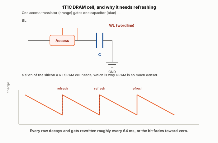
One transistor, one capacitor — dense and cheap, but the charge leaks.
One transistor and one capacitor, usually written as 1T1C, is a small fraction of what a 6T SRAM cell needs. That’s why we can pack DRAM into the gigabytes while SRAM stays stuck in the megabytes. But here’s the catch: capacitors leak. Even sitting there doing nothing, a DRAM cell’s charge drains away in just milliseconds. So the memory controller has to refresh every row on the chip, over and over, reading it and writing the same value straight back before it fades — usually a full pass across the whole chip about every 64 milliseconds. That’s where the word “dynamic” comes from. The bit only stays there because something keeps re-writing it.
One more thing worth knowing while we’re down here: reading a DRAM cell is actually destructive. Connecting that tiny capacitor to a much bigger bitline doesn’t just sense the charge, it disturbs it. A sense amplifier catches which way the voltage moved and cleans it back up to a proper logic level, but the cell’s own charge has already been knocked around, so every read gets followed by an automatic write-back. Reading and refreshing are, at the circuit level, almost the same operation.
So what did SDRAM actually change?
Here’s the part that surprises most people: when DRAM became SDRAM, the storage cell didn’t change at all. Still the same 1T1C capacitor. What changed was how the chip talks to the outside world.
The earliest DRAM chips were asynchronous — no shared clock between the chip and the memory controller. The controller would send a command, then just had to wait a fixed worst-case time before trusting the result. No overlap, no pipelining, because there was no shared timing reference to coordinate around.
Synchronous DRAM (SDRAM) fixed exactly that one problem. Add a shared clock line, and now the controller and the chip count the same ticks together. Once both sides agree on the beat, the controller can issue a new command every cycle while the last one is still finishing up internally, because everyone knows exactly which edge everything happens on. Nothing about the storage got faster or denser. The entire speedup came from replacing “wait for a timeout” with “hand off on a shared clock.”
So here’s the answer to a question you’ll hear a lot: SDRAM is not a competitor to DRAM. It’s the same DRAM cell, wearing a synchronous interface. And everything we’re about to cover is built on top of that same synchronous foundation.
DDR: how do you double the data rate without doubling the clock?
Plain SDRAM — what people now call SDR SDRAM, for Single Data Rate, now that DDR exists — sends one word of data per clock cycle, and only on the rising edge. DDR (Double Data Rate) SDRAM sends data on both the rising and the falling edge of the same clock. Same clock speed, twice the data.
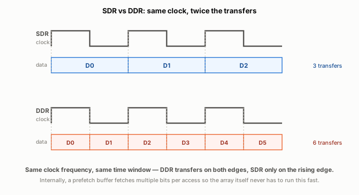
Same clock, twice the transfers — DDR moves data on both edges instead of one.
That sounds simple enough, but how does the chip actually pull it off? The internal memory array can’t just start running twice as fast because the pins are toggling twice as fast — the array itself is comparatively slow. So DDR fetches multiple bits internally in one go, parks them in a small buffer called the prefetch buffer, and then shifts them out the pins at the higher rate. The first DDR generation uses a 2n-prefetch: grab two bits internally for every one high-speed stream at the pins.
Every generation since has just doubled that internal parallelism again, so the pins can keep getting faster without asking the storage array to keep up:
| Generation | Prefetch | I/O bus width per DIMM | Core voltage | What changed |
|---|---|---|---|---|
| SDR SDRAM | 1n | 64-bit | 3.3 V | The synchronous baseline — one transfer per clock |
| DDR | 2n | 64-bit | 2.5 V | First “both edges” generation |
| DDR2 | 4n | 64-bit | 1.8 V | Doubled the internal parallelism again |
| DDR3 | 8n | 64-bit | 1.5 V | Same prefetch as DDR4, cleaner signaling |
| DDR4 | 8n | 64-bit | 1.2 V | Added bank groups for more parallel streams |
| DDR5 | 8n (×2 sub-channels) | Two independent 32-bit sub-channels | 1.1 V | Splits one DIMM into two independent halves |
Every row in that table is the same trick, just pushed one step further: fetch more bits in parallel internally, so the external pins can be fed faster without needing a faster core.
So, is DDR “a type of” SDRAM? Yes, plainly. The correct full name of the chip sitting in your PC is “DDR5 SDRAM” — DDR was never a rival to SDRAM, it’s SDRAM’s own lineage. When someone says DDR, the SDRAM part is already baked in. When old-timers say plain “SDRAM,” they usually mean the original, pre-DDR, single-data-rate version.
Why won’t a DDR5 stick fit in a DDR4 slot?
We already covered in the pillar article that generations don’t mix. Here’s the actual electrical reason, and it’s not arbitrary. Look at that voltage column again: 2.5 V down to 1.1 V across five generations. Higher data rates need lower voltages, both for signal integrity and to keep the chip from cooking itself. A DDR3 chip simply cannot run at DDR5 voltages.
So the little notch cut into the row of gold contacts on a DIMM is placed in a different spot for every generation, on purpose. It’s not a branding gimmick. It’s there so you physically cannot push a DDR4 stick far enough into a DDR5 slot to make contact — which stops you from ever feeding a chip the wrong voltage.
And where does SRAM fit into all this?
It doesn’t, and that’s worth noticing. Everything we just walked through — SDRAM, DDR, DDR2 all the way to DDR5 — is a DRAM-only story. SRAM never joined this progression, because it was never trying to solve the same problem. SRAM’s whole selling point is “ready instantly, no refresh, no prefetch games needed,” precisely because it has no capacitor quietly leaking in the background. That’s still exactly why it lives in CPU cache and small microcontroller RAM pools today, completely untouched by whichever DDR generation your main memory happens to be running.
What’s next
GPUs take this exact same DDR SDRAM lineage and twist it toward a completely different goal: raw bandwidth instead of quick single-request latency. That split is where GDDR and HBM come from, and that’s the whole subject of the next article: DDR vs GDDR vs HBM: How GPU Memory (VRAM) Actually Works.