DDR vs GDDR vs HBM: How GPU Memory (VRAM) Actually Works
In the memory map article, I told you VRAM is just DRAM that belongs to the GPU. True, but it skips the actually interesting question: DRAM, sure, but which DRAM, and why can’t a graphics card just use the same DDR sticks your motherboard uses?
The DDR article showed you that DDR, DDR2, all the way through DDR5, are one lineage built to solve one problem: answer a CPU core fast, one request at a time. A GPU has a completely different problem. So it grew two completely different memory families out of that same DDR foundation — GDDR and HBM. Let’s see why.
It’s not about speed. It’s about shape.
Picture what a CPU core actually does. It runs through one instruction stream, and a lot of those instructions depend on the result of the one before it. So what does that core need from memory? A fast answer to one request. That’s latency, and it’s the thing DDR was built to chase.
Now picture a GPU. Thousands of small cores, all chewing through mostly-independent work at the same time — shading a few million pixels, transforming a few million vertices — mostly by streaming big, predictable blocks of data like textures and frame buffers. What does that workload actually need? Not a fast answer to one request. A huge number of requests all being served at once. That’s bandwidth, and a GPU can shrug off a slow answer to any single request, because there are thousands more already queued up to keep those cores busy while it waits.
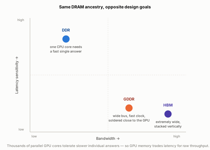
Same DRAM ancestry, opposite design goals: CPU memory chases latency, GPU memory chases bandwidth.
That one difference — one request fast, versus thousands of requests at once — is the entire reason GDDR and HBM exist. Neither one is “better” DRAM than DDR. They’re DDR’s own family, just re-engineered around a much wider, much more parallel, much more patient workload.
GDDR: same DDR trick, wired for bandwidth instead of flexibility
GDDR (Graphics DDR) starts from the exact same double-data-rate, prefetch-buffer trick you already saw in the DDR article. What changes is how it’s physically wired into the system, and every change points the same direction: trade flexibility for bandwidth.
- A wider bus per chip. Your system DDR chip talks over a narrow ×4, ×8, or ×16 interface, because it has to be one of many chips sharing a bus that works across different motherboards and different DIMM counts. A GDDR chip never has to be that flexible — it’s soldered to one board, wired to one GPU, forever — so it goes wide instead, typically 32 bits per chip.
- Soldered, not socketed. No DIMM slot, no connector. That means shorter, cleaner, more consistent traces between the memory chip and the GPU die. Shorter and cleaner tolerates a much faster signal than a connector reaching across multiple slots ever could.
- Room to run hot. A handful of GDDR chips ringing a GPU die sit right next to that GPU’s own beefy cooler. So they get to run hotter and pull more power per bit than a DIMM stick stuck in a case with modest airflow.
Every GDDR generation just pushes those same three levers further. GDDR6X added one genuinely new trick worth knowing, though: PAM4 signaling. A normal signal (called NRZ) can only be high or low, so one transition carries one bit. PAM4 uses four distinct voltage levels instead of two, so one transition carries two bits — you get double the information without touching the clock speed at all. GDDR7 pushes it even further with PAM3 encoding, plus independent sub-channels similar to what DDR5 did.
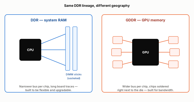
Same lineage, different geography: DDR reaches across slots, GDDR never leaves the board.
HBM: don’t go wide across the board — go up
HBM (High Bandwidth Memory) chases the same bandwidth goal, but takes the opposite path to get there. Instead of widening a flat bus and cranking the clock, HBM stacks several DRAM dies vertically, drills thousands of microscopic connections straight through them called through-silicon vias (TSVs), and drops the whole stack onto a silicon interposer sitting right beside the GPU die. This whole approach even has a name: 2.5D integration — the stack and the GPU sit side by side on a shared silicon carrier, instead of the cheaper fiberglass board GDDR chips get soldered onto.
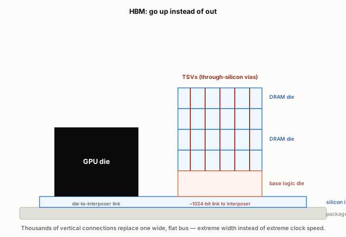
HBM goes up instead of out — stacked dies, thousands of vertical connections, sitting inches — not centimeters — from the GPU.
So why bother stacking dies instead of just wiring a wider bus? Because that stack of TSVs gives each HBM package an interface that’s staggeringly wide — around 1024 bits per stack, against 32 bits for one GDDR chip — and once your bus is that wide, no individual connection has to hurry. GDDR gets its bandwidth by clocking a moderately wide bus very fast. HBM gets the same bandwidth the other way: make the bus so wide that speed per pin barely matters. And the interposer is what makes this practical at all, since it keeps every one of those thousand-plus connections microscopically short.
None of this comes free, though. TSVs, interposers, precision die-stacking — these are exacting, expensive manufacturing steps next to just soldering a chip onto a normal board. That’s the whole reason you find HBM on data-center AI accelerators and the very top of the workstation GPU stack, while GDDR stays the default everywhere board cost actually matters — which is to say, everywhere you’d actually shop for a graphics card.
Putting the numbers side by side
| DDR5 (system RAM) | GDDR6X | HBM3 | |
|---|---|---|---|
| Interface width | 2× 32-bit sub-channels per DIMM | 32-bit per chip | ~1024-bit per stack |
| Typical bandwidth | ~40–50 GB/s per DIMM | ~80–100+ GB/s per chip | ~800 GB/s–1.2+ TB/s per stack |
| Physical form | Socketed DIMM stick | Chips soldered around the GPU die | Dies stacked vertically on an interposer beside the die |
| Optimized for | Low latency, flexibility, upgradability | High bandwidth at moderate cost | Maximum bandwidth per watt and per millimeter |
| Typical home | Desktops, laptops, servers | Consumer and prosumer GPUs | AI accelerators, top-tier compute GPUs |
Treat these as generation-typical figures, not a spec sheet for any one product — they’ll shift with every new generation on all three rows. What matters is the shape of the comparison, not the exact numbers.
So what actually is VRAM?
Here’s the payoff, after all that: “VRAM” was never a technology. It’s a role. It just means “whatever DRAM is dedicated to the GPU.” Depending on which GPU you’re holding, the chip filling that role could be GDDR (the overwhelming majority of consumer graphics cards), HBM (AI accelerators, plus a handful of high-end consumer cards — AMD’s Radeon VII and the Fury/Vega lineup were the well-known examples), or — more and more often — nothing dedicated at all.
That last case matters more every year. Integrated graphics, and designs like Apple’s unified memory (which the pillar article covers), skip dedicated VRAM entirely. The GPU just shares the same pool of system DDR or LPDDR the CPU is already using, trading some peak bandwidth for zero-copy convenience and a simpler system design. There’s no VRAM chip to point at in that design — just one memory pool doing two jobs.
So here’s the rule of thumb to actually use when you’re buying: more VRAM capacity — almost always GDDR, on anything you’d realistically shop for — is what lets a card hold higher resolutions and heavier texture settings comfortably in memory. HBM’s edge is bandwidth density and power efficiency at extreme scale, which matters when you’re training large models across a rack of accelerators. It has basically nothing to do with whether your game stutters at 4K — GDDR has had that job covered for two decades.